AVR-Based Datalogger
In the previous chapter, we saw how to design a datalogger based on a PIC16F873A. A datalogger based on an AVR is not too dissimilar. Figure 15-11 shows the basic schematic.
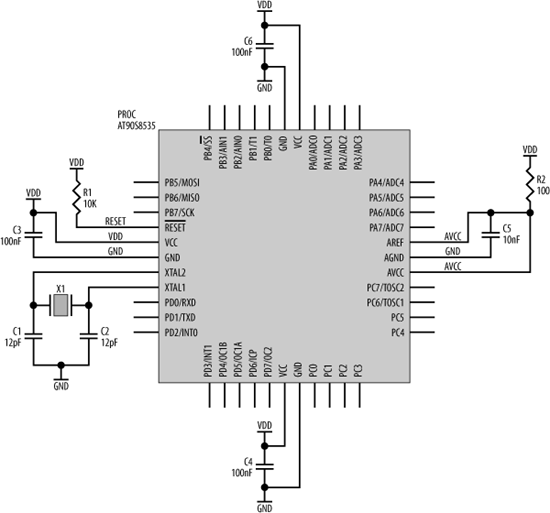
The connections for interfacing a serial dataflash memory chip to an Atmel 90S4434 AVR processor are simply SPI, as with the PIC processor. The AVR portion of the schematic is no different from the examples we have seen previously. That's the nice thing about simple interfaces such as SPI. They form little subsystem modules that "bolt together" like building blocks. Start with the basic core design and just add peripherals as you need them. The schematic also shows decoupling capacitors for the power supplies, the crystal oscillator for the processor, and a pull-up resistor for ![]() . Pin 41 (PB1) is used as a "manual" (processor-controlled) reset input to the flash.
. Pin 41 (PB1) is used as a "manual" (processor-controlled) reset input to the flash.
The analog inputs, ADC0:ADC7, can be connected to an IDC header allowing for external sampling, or they can be interfaced directly to sensors, as we saw with the PIC datalogger. The serial port signals, RXD and TXD, connect to a MAX3233 in the same way as we saw in the PIC design.

Figure 15-10. AT90S8535 processor and support components
Get Designing Embedded Hardware, 2nd Edition now with the O’Reilly learning platform.
O’Reilly members experience books, live events, courses curated by job role, and more from O’Reilly and nearly 200 top publishers.

