21Temporary Carrier Technologies for eWLB and RDL‐First Fan‐Out Wafer‐Level Packages
Thomas Uhrmann and Boris Považay
EV Group – St. Florian am Inn, Austria
Fan‐out wafer‐level packaging (FO‐WLP) process flows typically fall under two basic integration categories called chip‐first and chip‐last. With the chip‐first approach, individual chips are embedded into epoxy mold, forming freestanding molded wafers as a basis for redistribution layers (RDL) and bumping, referred to as embedded wafer‐level ball grid array (eWLB). In the chip‐last approach, RDL are processed first, before the die are individually attached and overmolded. In both process flows as shown in Figure 21.1, temporary wafer carrier technologies play a crucial role. For chip‐first (or RDL‐last), temporary carriers are used for package‐on‐package (PoP) technology, where thinning device wafers below 400 μm does not allow for the use of freestanding molded wafer handling, as discussed by Campos et al. [1–3]. Slide‐off debonding has been found to work reliably within the molded wafer process flow.
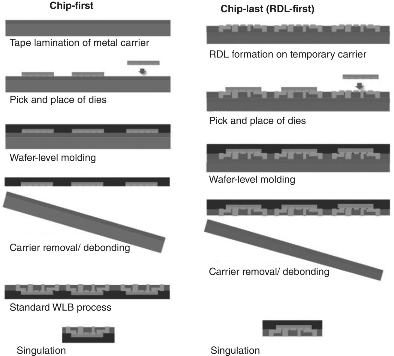
Figure 21.1 Schematic manufacturing process for chip‐first and chip‐last integration, including the use of temporary carriers.
For eWLB, the warpage of the molded substrates is generally one of the biggest challenges for high volume manufacturing. The different coefficient of thermal expansion (CTE) for silicon and ...
Get Advances in Embedded and Fan-Out Wafer Level Packaging Technologies now with the O’Reilly learning platform.
O’Reilly members experience books, live events, courses curated by job role, and more from O’Reilly and nearly 200 top publishers.

