19Equipment and Process for eWLB: Required PVD/Sputter Solutions
Chris Jones1, Ricardo Gaio2, and José Castro2
1 SPTS Technologies Ltd, Newport, UK
2 Amkor Technology Portugal S.A., Portugal
19.1 Background
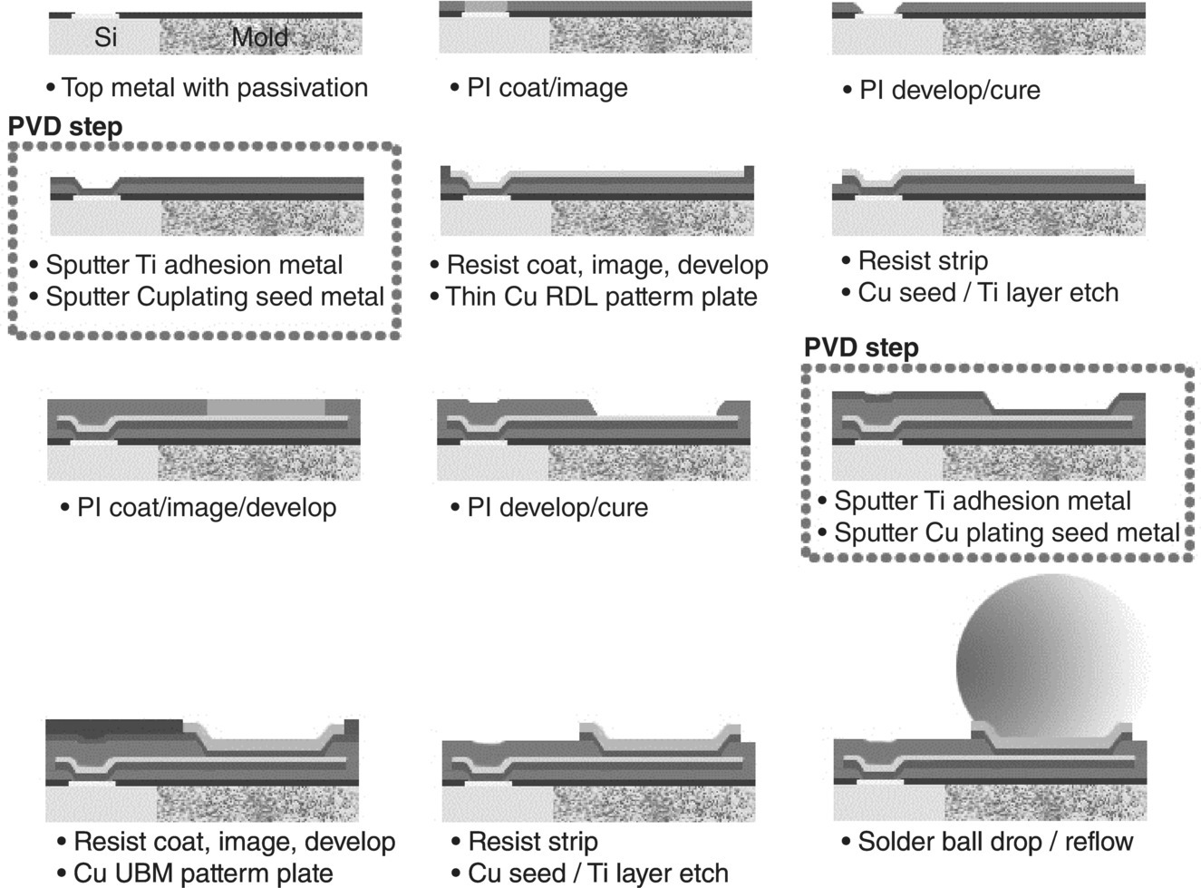
In a fan‐out WLP (FO‐WLP) structure, conducting redistribution layers (RDL) are formed in dielectric material to relocate device input and output (I/O) electrical connection points to different areas of a die surface, to areas of mold real estate around the periphery, or even to link adjacent die embedded in mold, depending on the packaging structure and application. Many layers of RDL with vias connecting each layer are used when I/O density is high to avoid interconnect congestion. They are formed in photosensitive resist materials following the basic process flow illustrated in Figure 19.1.

Figure 19.1 RDL process flow.
For multilevel RDL structures, the RDL formation process is repeated, depending on the number of conductive routing layers required, with the final plating pass acting as an under‐bump metal (UBM) layer prior to solder or ball drop connection.
RDL conductor metal is predominantly copper (Cu) deposited using electrochemical deposition (ECD). ECD requires a thin conducting seed layer to initiate the ECD process. Cu is typically used in combination with an adhesion layer underneath, often titanium (Ti) or titanium–tungsten (TiW). The industry standard ...
Get Advances in Embedded and Fan-Out Wafer Level Packaging Technologies now with the O’Reilly learning platform.
O’Reilly members experience books, live events, courses curated by job role, and more from O’Reilly and nearly 200 top publishers.

