9Embedding of Active and Passive Devices by Using an Embedded Interposer: The i2 Board Technology
Thomas Gottwald, Christian Roessle, and Alexander Neumann
Schweizer Electronic AG, Schramberg, Germany
9.1 Technology Description
Currently, there are two major trends in embedding technology: embedding for system in package (SiP), which is supposed to be assembled onto commodity printed circuit boards (PCB), and system in board (SiB), where the embedding of components takes place in the main board (see Figure 9.1). The i2 Board is an embedding technology for SiB.
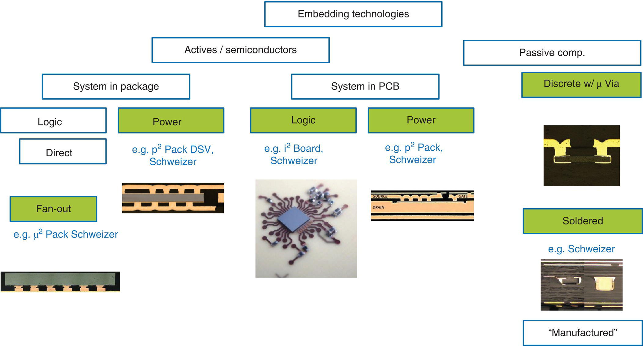
Figure 9.1 Overview of embedding technologies.
The major difference between i2 Board and other embedding technologies is that i2 Board is a fan‐out packaging technology. The i2 Board technology was developed to enable chip embedding of fine‐pitch chips with high input and output signal (I/O) count into the main boards. The i2 Board approach uses an interposer to simplify the mechanical and electrical connection between chip and PCB. This has a significant positive influence on cost, ease of supply chain, testability, and the feasibility for chips with fine pitches. An example of an assembled interposer can be seen in Figure 9.2.
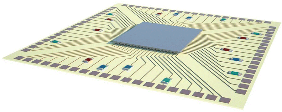
Figure 9.2 Active and passive components assembled on i2 Board interposer before embedding. ...
Get Advances in Embedded and Fan-Out Wafer Level Packaging Technologies now with the O’Reilly learning platform.
O’Reilly members experience books, live events, courses curated by job role, and more from O’Reilly and nearly 200 top publishers.

